Stran trenutno ni na voljo v vašem jeziku. Lahko si ogledate strojni prevod, ustvarjen s storitvijo Google Translate. Te storitve ne zagotavljamo mi in rezultatov prevoda nismo preverili.
Za dodatno pomoč se lahko obrnete na nas.
Carbon, 2D materials and nanotechnology
The massive range of consumer products that use carbon-based materials—and the promise of 2D materials for future technologies—make these key application areas for Raman spectroscopy.
You can use Raman to identify all the forms of carbon, including graphene, carbon nanotubes (CNT), graphite, diamond, and diamond-like carbon (DLC). You can also study 2D materials such as MoS2, hBN, and WSe2.
Analyse all forms of carbon
Renishaw's Raman systems are being used to research, develop, and control the quality of carbon materials. You can determine:
- the number of graphene layers, and their defects, doping and strain
- Diamond Like Carbon (DLC) thickness and hybridised composition (sp2 and sp3)
- Carbon Nanotube (CNT) diameter and functionalisation
- diamond stress, purity and origin (synthetic or natural)
- the properties of C60 and other fullerenes
- the structural composition of amorphous carbons
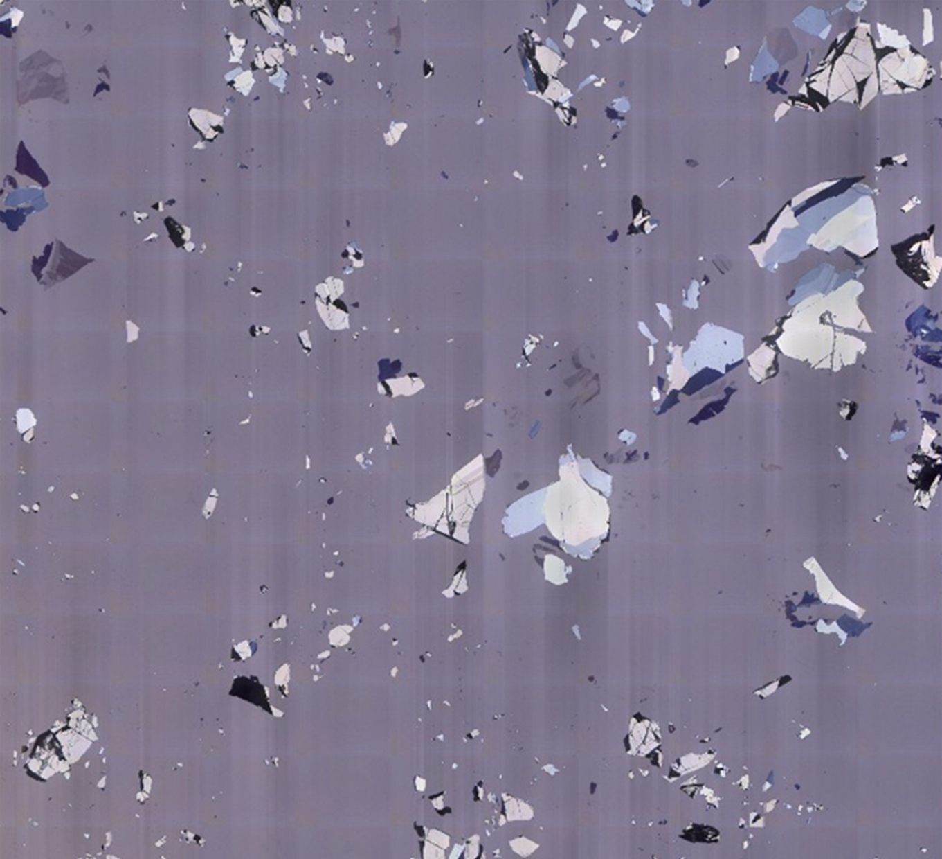
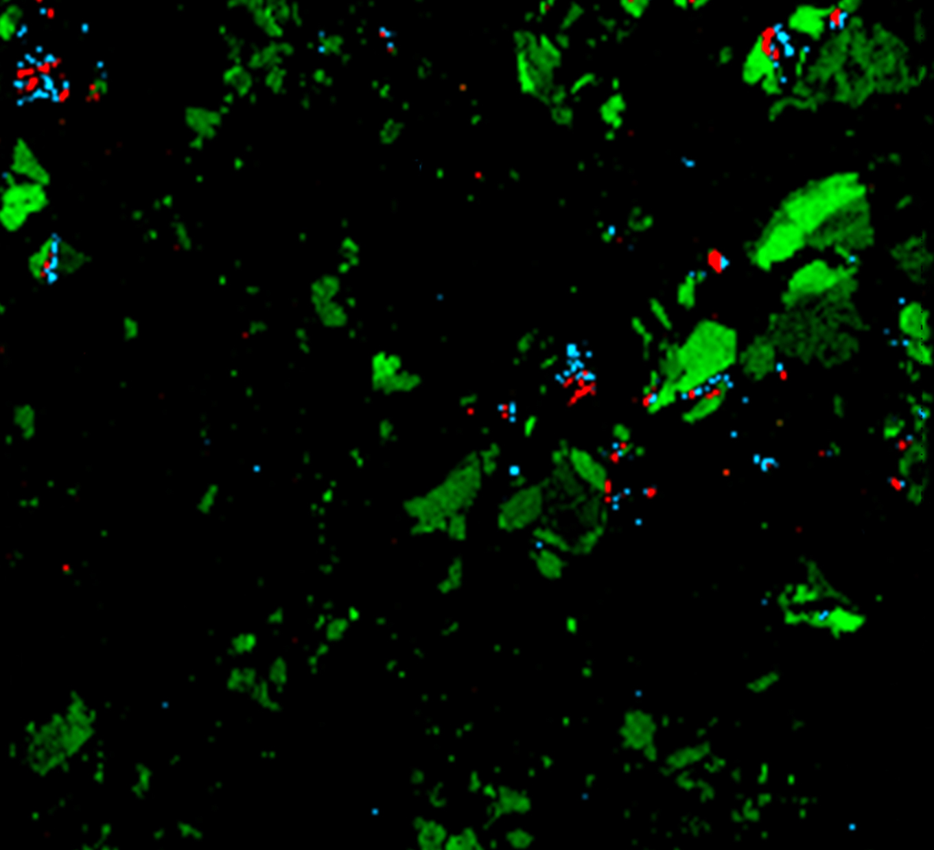
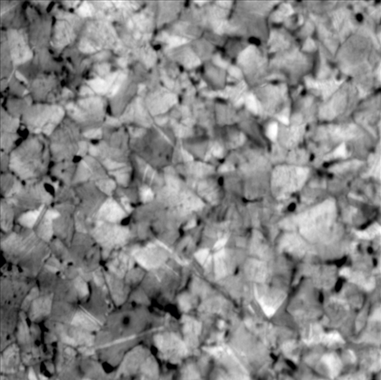

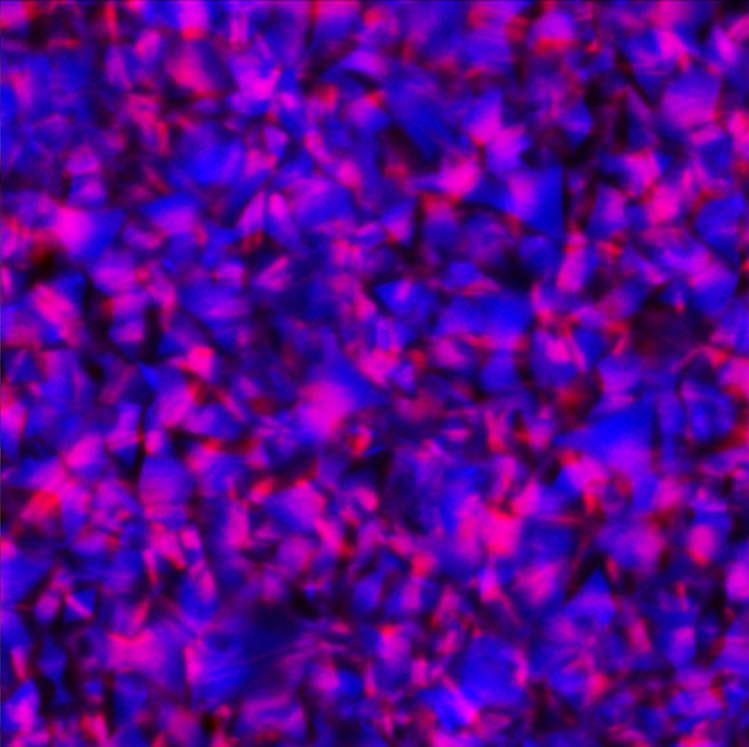
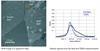
Raman and photoluminescence images of a hot-filament-grown CVD diamond film.
The Raman image indicates the intensity of the 1332 cm-1 diamond band. Darker regions have higher graphitic content; this leads to lower laser penetration and a weaker diamond signal.
The photoluminescence image is based on the intensity of the 1.77 eV band (red, most likely related to contamination from the filament during growth) and the intensity of the 1.95 eV band (blue, [N-V]- nitrogen vacancy).
Monolayers and thin films
The massive range of consumer products that use carbon-based materials—and the promise of 2D materials for future technologies—make these key application areas for Raman spectroscopy.
Some of these new materials consist of single, or just a few, atomic layers. The high sensitivity of Renishaw's Raman systems makes identifying and analysing them quick and easy.
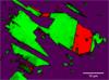
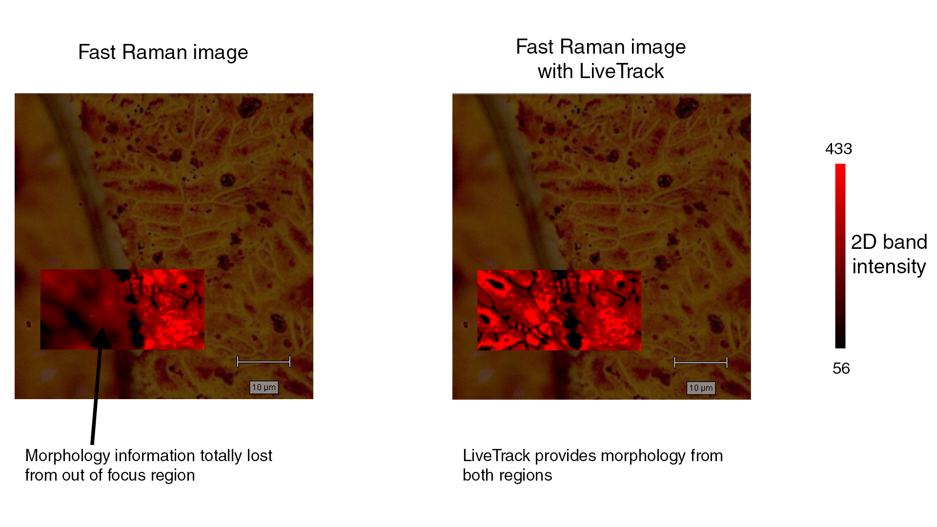
Analyse CVD graphene grown on copper foils
Renishaw's LiveTrack™ focus-tracking technology maintains sample focus, even when mapping large areas that are not flat.
More signal, no damage
Some thin carbon films, such as DLC, can be damaged by high laser power densities. With Renishaw's line-focus laser illumination technology, power densities are reduced, but total laser power is retained. You can collect high quality data rapidly, without damaging your samples.
Nanotechnology
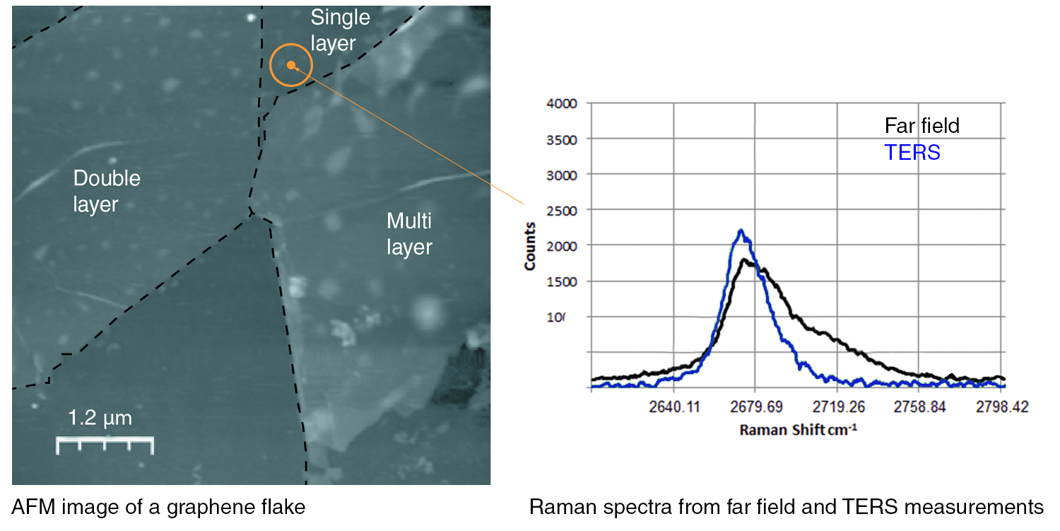
The high spatial resolution of Renishaw's inVia confocal Raman microscope makes it suitable for studying the structure and defects of nanomaterials, such as graphene and CNTs.
Renishaw can combine Raman analysis with scanning probe microscopes (such as atomic force microscopes). These systems add chemical analysis capabilities to the high spatial resolution topography and property information acquired by SPMs/AFMs. You can also use tip-enhanced Raman spectroscopy (TERS) to acquire nanometre-scale Raman chemical information.
All encompassing spectra
Renishaw's SynchroScan produces high-resolution wide-range spectra. Collecting data covering the entire Raman and photoluminescence range is simple and fast. For example, you can:
- see carbon nanotube radial-breathing modes (RBMs), with the G and 2D bands, together
- study photoluminescence features associated with defects in diamond, as well as its Raman spectrum
We're here when you need us
To find out more about this application area, or an application that isn't covered here, contact our applications team.
Contact our applications team
Downloads: materials science (carbon, 2D materials and nanotechnology)
-
 Application summary: Raman measurements on graphene
The high specifity of inVia enables graphene to be easily differentiated from other materials, including carbon allotropes such as carbon nanotube and diamond.
-
 Application note: Analyse 2D materials with the inVia Qontor confocal Raman microscope
With so many unique properties, working with 2D materials can be challenging. Whether it is large regions, uneven samples, or small discrete flakes, Renishaw’s inVia Qontor confocal Raman microscope gives you reliable results, quickly and easily.
-
 Product note: Rayleigh imaging using the inVia™ confocal Raman microscope
Product note detailing how you can perform Rayleigh imaging on the inVia confocal Raman microscope.

Watch our joint webinar with Oxford Instruments
Growth & Characterisation of 2D Materials Beyond Graphene
Investigation into the physics and technology of graphene in the past decade has triggered research into a large family of similar Van der Waals structures.
One such class of materials that is receiving a huge amount of attention is Transition Metal DiChalcogenides (TMDCs) which have shown immense potential towards both electronics and optoelectronics applications. This webinar will focus on recent advances in growth of 2D materials and on Raman characterisation, and elucidate the interplay between process engineering and materials characterisation.
The webinar comprises two talks:
Characterisation of 2D materials and heterostructures - Dr Tim Batten, Renishaw, UK
Deposition of 2D materials and heterostructures - Dr Ravi Sundaram , Oxford Instruments, UK
Related stories
The world's lightest mechanical watch
In January 2017, the world's lightest mechanical chronograph watch was unveiled in Geneva, Switzerland, showcasing an innovative composite material containing graphene. Now the research behind the project has been published with the Renishaw inVia Raman microscope playing an important role in the development of the material.
Quality control analysis at New Plasma Technologies
New Plasma Technologies (NPT), based in Moscow, Russia, uses a Renishaw inVia confocal Raman microscope for investigating the structure and chemical properties of materials, non-destructively.